Case Detail
PCB Design Cases
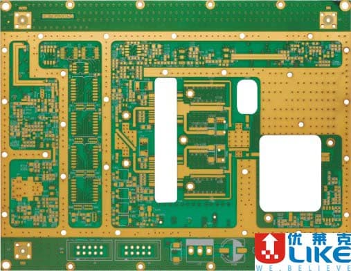
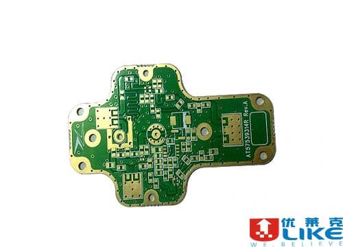
High-frequency PCB Board
High-frequency PCB Board is a PCB engineering reference project from ULIKE. The case highlights schematic review, layout optimization, stack-up planning, impedance-aware routing, and manufacturability checks, with original process notes covering 1表面工艺:喷锡、无铅喷锡、沉金、全板镀金、插头镀金、化学沉锡(银)、抗氧化(OSP)蓝胶、碳油.
Ask About Similar ProjectsProcess notes
- 1表面工艺:喷锡、无铅喷锡、沉金、全板镀金、插头镀金、化学沉锡(银)、抗氧化(OSP)蓝胶、碳油
- 2多层板能批量生产2层至10层,6层和8层HDI板子可小量生产。
- 3最小线宽/间距:3mil/3mil BGA间距:0.25MM左右(三星6410)
- 4成品最小孔径:0.1mm
- 5最大尺寸:610mmX1200mm
- 6油墨:日本Tamura、Taiyo感光油墨;
Delivery attention
- Provide mechanical limits, connector positions and keep-out areas before layout starts.
- Confirm stack-up, impedance and key signal requirements early to reduce board revision.
- Before fabrication, review Gerber, drill, paste mask and assembly drawings together.
Project record
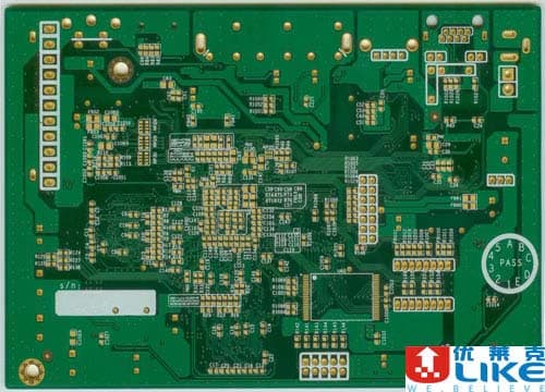
ULIKE used this high-frequency pcb board case to demonstrate practical PCB design support for manufacturable layouts, faster prototype cycles, and engineering documentation. Key technical notes include: 1表面工艺:喷锡、无铅喷锡、沉金、全板镀金、插头镀金、化学沉锡(银)、抗氧化(OSP)蓝胶、碳油; 2多层板能批量生产2层至10层,6层和8层HDI板子可小量生产。; 3最小线宽/间距:3mil/3mil BGA间距:0.25MM左右(三星6410); 4成品最小孔径:0.1mm; 5最大尺寸:610mmX1200mm; 6油墨:日本Tamura、Taiyo感光油墨;.
The work is suitable for OEM and ODM customers that need a reliable partner from engineering review through production handoff.
Image record
Photos are kept as production and project references.