Case Detail
PCB Design Cases
High-speed PCB Design In PADS
High-speed PCB Design In PADS is a PCB engineering reference project from ULIKE. The case highlights schematic review, layout optimization, stack-up planning, impedance-aware routing, and manufacturability checks, with original process notes covering 24小时快速交货.
Ask About Similar ProjectsProcess notes
- 24小时快速交货
- 先进技术产品
- 高层背板、HDI板、高频板、高TG板、无卤素板、挠性及刚挠板等高新技术产品
- 16层PCB,2mil线宽间距
- 产品与技术应用
Delivery attention
- Provide mechanical limits, connector positions and keep-out areas before layout starts.
- Confirm stack-up, impedance and key signal requirements early to reduce board revision.
- Before fabrication, review Gerber, drill, paste mask and assembly drawings together.
Project record
ULIKE used this high-speed pcb design in pads case to demonstrate practical PCB design support for manufacturable layouts, faster prototype cycles, and engineering documentation. Key technical notes include: 24小时快速交货; 先进技术产品; 高层背板、HDI板、高频板、高TG板、无卤素板、挠性及刚挠板等高新技术产品; 16层PCB,2mil线宽间距; 产品与技术应用; 双面快件24小时内提供; 2-4天内可提供十层以内样板;十层以上产品一周内交货.缩减新产品研发周期,占领市场先机,ulikepcba为研发量身订做; 10年来不断研究PCB加工技术,大力引进海外生产制造设备,我们使用激光直接成像系统、高层板层压系统及系统的在线品质控制令目前加工能力已经可以稳定生产16层PCB及20层刚挠结合板。背板板厚可超过7mm(0.276″),厚径比可达到22:1;高精密可制作2mil线宽间距,并掌握阻抗控制技术,实现您的高速信号传输设计。; 合作伙伴.
The work is suitable for OEM and ODM customers that need a reliable partner from engineering review through production handoff.
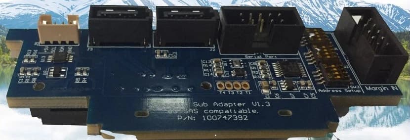
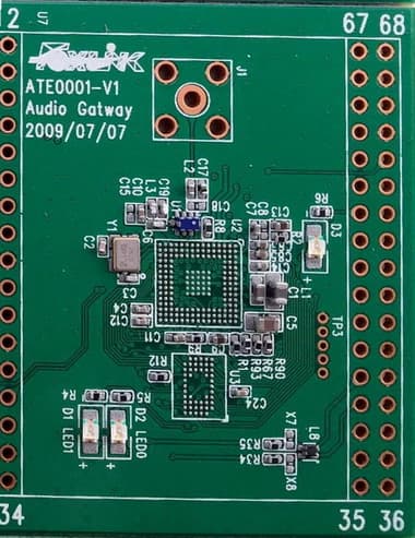
Image record
Photos are kept as production and project references.